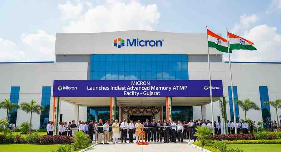
Sanand Semiconductor Plant Ships First DRAM Module, Boosts India’s Chip Ambitions
India advanced its semiconductor roadmap as Micron Technology began operations at its advanced memory ATMP facility in Sanand, Gujarat. Inaugurated by Narendra Modi , the plant dispatched its first finished DRAM module to Dell Technologies , marking India’s entry into high-end semiconductor assembly and testing.
World-Scale Clean Room Infrastructure
The Sanand unit features a 500,000 sq ft raised-floor clean room—among the largest single semiconductor assembly clean rooms globally. Designed for Gujarat’s geotechnical and climatic conditions, the structure controls moisture and vibration risks. Rated Class 1000, it limits airborne particles to stringent thresholds, with air recirculated up to 120 times per hour to safeguard ultra-fine bonding wires and integrated circuits.
Advanced Memory Operations
The facility performs Assembly, Testing, Marking and Packaging (ATMP) for DRAM and NAND flash memory. DRAM powers computing workloads in PCs, smartphones and data centres, while NAND provides non-volatile storage in SSDs and devices. Under a wafer-in to finished-product-out workflow, wafers from global fabs are thinned, diced, packaged, tested and mounted onto modules before final quality assurance.
Planned investment across phases totals about $2.7 billion. Output is set to scale from tens of millions of units this year toward nearly one billion annually by 2027, serving both export and domestic markets. Initial shipments include DRAM modules for Dell, with supplies envisaged for firms such as Asus and Qualcomm.
Workforce and Technology Stack
The plant employs ~1,300 personnel, with targeted semiconductor curricula and overseas training in Malaysia and Singapore. Automation, AI-driven factory analytics and advanced yield tools align the site with global manufacturing benchmarks.
Important Facts for Exams
-
ATMP = Assembly, Testing, Marking and Packaging.
-
DRAM is volatile primary memory; NAND is non-volatile storage.
-
Clean room classes specify permissible particle counts per air volume.
-
Semiconductor value chain: design → fabrication → assembly/testing → packaging.
The Sanand ATMP strengthens India’s electronics value chain, reducing import dependence and advancing resilient semiconductor manufacturing.
Month: Current Affairs - Mar 03, 2026
Category: Semiconductor | Electronics Manufacturing