leap from conventional organic packaging, offering better thermal performance and higher integration density critical for AI-grade chips.
Government Support and Funding
The Government of India is providing strong support under the India Semiconductor Mission (ISM). Central government fiscal support is Rs 799 crore, and additional state support is about Rs 399.5 crore. The total project cost is estimated at Rs 1,943.53 crore. The Union Minister said the agreement aligns with the government's vision of developing a full semiconductor manufacturing ecosystem in India. He cited the entry of firms such as Applied Materials, Lam Research, Tokyo Electron, Merck Electronics and the Tata Electronics–ASML partnership as evidence of growing global confidence in India's semiconductor sector.
Odisha's Growing Semiconductor Hub Status
Odisha is emerging as a major semiconductor destination. Chief Minister Mohan Charan Majhi said the state is the only state in the country where both India's first compound semiconductor fabrication unit and first 3D glass substrate packaging facility are being established. The state has already received investments worth over Rs 10,000 crore in the semiconductor sector. Companies like SiCSem Private Limited, in collaboration with UK-based Clas-SiC Wafer Fab Ltd., are setting up India's first commercial compound semiconductor fabrication unit in Info Valley, with groundbreaking scheduled for June 2026. Chief Secretary Anu Garg said, "With strong policy support, skilled talent and integrated infrastructure, Odisha is ready to contribute meaningfully to India's semiconductor ambitions".
Applications and Future Outlook
The products manufactured at these units will serve high-growth sectors including artificial intelligence, high-performance computing, defence electronics, next-generation telecom systems, automotive, renewable energy and electric vehicles. Babu Mandava, CEO of 3D Glass Solutions, said the initiative has the potential to establish India as a key global hub for advanced glass substrates and semiconductor packaging. Naga Chandrasekaran, Executive VP and GM of Intel Foundry, said Intel is "excited about the potential of this collaboration to accelerate the commercialization of next-generation advanced packaging solutions globally". The development is aligned with Odisha's Vision 2036 and India's vision of Atmanirbhar Bharat, positioning Odisha at the forefront of the global digital economy.
Exam-Focused Points
-
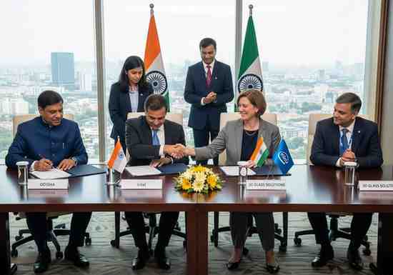
MoU signed between: Odisha government, Intel Corporation and 3D Glass Solutions Inc. (USA).
-
Dates of signing: 28 and 29 May 2026.
-
Witnesses: Ashwini Vaishnaw (Union Electronics & IT Minister), Mohan Charan Majhi (Odisha CM), Lip-Bu Tan (Intel CEO).
-
Investment: $3.3 billion (approximately).
-
Location: Bhubaneswar-Khurda region, Odisha (Info Valley).
-
Project cost of 3DGS unit: Rs 1,943 crore (central fiscal support: Rs 799 crore, state support: Rs 399.5 crore).
-
Annual production capacity: ~70,000 glass panel substrates, 50 million assembled units, ~13,000 3DHI modules.
-
Employment generation: 1,800+ direct high-skilled jobs + significant indirect jobs.
-
Project timeline: Phased implementation over 5-6 years; commercial production by August 2028.
-
Intel's role: Technology partner providing know-how, process expertise, licensing, quality systems, and workforce training.
-
India Semiconductor Mission
Month: Current Affairs - May 30, 2026
Category: Intel3DGS